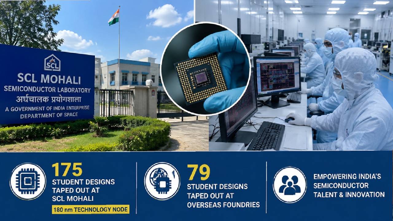
In a major milestone for India’s rapidly growing semiconductor sector, the Semi-Conductor Laboratory (SCL), Mohali, has successfully completed the tape-out of 175 semiconductor chip designs developed by engineering students using its 180-nanometre (180 nm) CMOS fabrication technology. The achievement marks one of the country’s largest academic semiconductor fabrication initiatives and highlights SAS Nagar Mohali’s growing importance as a key centre for semiconductor research, chip design, and advanced electronics manufacturing.
The successful tape-out signifies that all 175 student-designed integrated circuits (ICs) have successfully completed the critical stages of design, simulation, verification, and validation before moving to the fabrication process. Tape-out is regarded as one of the most important milestones in semiconductor development, as it represents the final approved design that is transferred for manufacturing on silicon wafers.
Adding to this achievement, 79 additional chip designs developed by Indian students have also been successfully taped out at international semiconductor foundries, reflecting the rapid advancement of India’s semiconductor design ecosystem. Together, these accomplishments demonstrate the country’s growing capabilities in Very Large Scale Integration (VLSI) design, integrated circuit engineering, and indigenous semiconductor innovation.

Punjab Government Schools Get New Focus Under Mann Government’s Education Reforms
Punjab News: Government schools across Punjab have witnessed significant changes in recent years as the state government has…
Continue readingThe student chip designs were developed through collaborative efforts involving leading engineering institutions, research organisations, and national semiconductor programmes dedicated to strengthening India’s semiconductor talent pipeline. Through these initiatives, students received access to industry-standard Electronic Design Automation (EDA) tools, advanced chip design software, fabrication infrastructure, and technical mentorship from semiconductor experts, enabling them to gain practical experience in designing production-ready integrated circuits.
Located in Sector 72, SAS Nagar Mohali, the Semi-Conductor Laboratory (SCL) is India’s premier government-owned semiconductor fabrication facility. Operating on 180 nm CMOS technology, the laboratory has played a strategic role in supporting critical sectors such as space, defence, telecommunications, healthcare, electronics, scientific research, and national security through indigenous semiconductor development and fabrication capabilities.
Technology experts believe that providing students with opportunities to design and fabricate real semiconductor chips significantly strengthens India’s future semiconductor workforce. Exposure to the complete semiconductor development cycle—including circuit design, simulation, verification, physical layout, fabrication, and testing—helps engineering students acquire practical industry skills that are increasingly in demand across the global semiconductor industry.
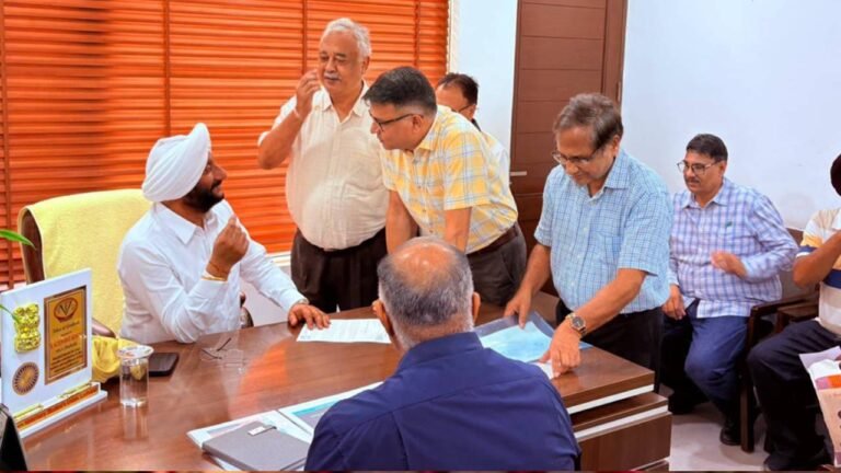
Kulwant Singh Interacts with Residents, Assures Resolution of Genuine Public Issues
Mohali: MLA Kulwant Singh met residents from different parts of the Mohali constituency during a public interaction programme…
Continue readingThe achievement also aligns with the Government of India’s Semiconductor Mission and the broader vision of building a self-reliant semiconductor ecosystem under national initiatives aimed at expanding domestic chip manufacturing, semiconductor design, electronics production, and research capabilities. Institutions like SCL Mohali are expected to play a pivotal role in developing highly skilled semiconductor professionals while supporting India’s long-term technological self-reliance.
The increasing participation of universities and engineering colleges in semiconductor design programmes reflects the growing interest among students in specialised fields such as VLSI design, embedded systems, artificial intelligence hardware, communication technologies, Internet of Things (IoT), automotive electronics, and advanced computing systems. These disciplines form the foundation of next-generation electronic products and digital technologies.
Industry specialists have welcomed the initiative, stating that stronger collaboration between academic institutions and semiconductor fabrication facilities helps bridge the gap between classroom education and industrial requirements. Such partnerships encourage innovation, accelerate research, and provide students with valuable exposure to real-world semiconductor manufacturing processes while strengthening India’s innovation ecosystem.
With India’s semiconductor industry witnessing unprecedented investment and policy support, SAS Nagar Mohali continues to establish itself as one of the country’s leading centres for semiconductor research, chip design, fabrication, and advanced electronics development. The successful tape-out of 175 student-designed semiconductor chips at SCL Mohali represents another significant milestone in India’s journey towards becoming a globally competitive semiconductor hub while further reinforcing Mohali’s position as a major destination for high-technology innovation, research excellence, and indigenous semiconductor manufacturing.



Comments